Development of Signal Analyzer Based on FPGA
Educational experimental tools of any institute of higher education is enough conservative by reason of financial limits. It is complicated to create laboratory lessons without expensive gaging equipment. The neediest devices in most cases are digital voltmeter, oscillograph and spectrum analyzer. Usually measuring equipment produced for industry needs have surplus functionality that makes them more expensive. Also it is hard to modernize such equipment.
In majority of electronic educational disciplines it is enough to use four-channel oscillograph with measuring band equals to 1 MHz to conduct laboratory lessons. Here some channels of oscillograph can be used like voltmeters. It is more practical to design measuring equipment by means of USB device that could be easily connected to personal computer (PC). This also makes it cheaper. In this case it is allowed to:
- simplify digital processing of signal,
- save up measurement results,
- easily extend the functionality of device,
- adapt device for concrete disciplines.
Developed device – digital signal analyzer – must be able to measure signals in spectrum and time domains, statistic characteristics and parame-ters of signal like density of probability distribution, average of distribution and dispersion.
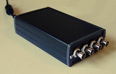
In the laboratory of electronic means of education in the Siberian state university of telecommunications and informatics (SibSUTIs) were developed universal measuring device – USB analyzer of signals based on FPGA.

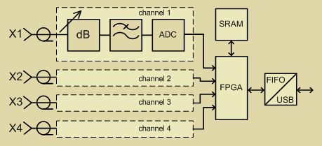
The add-on device has four symmetric analog input channels. Measurable signal gets on steerable attenuator that provides high input impedance (1 MOhm). Attenuator realizes switching of measurement limits and changing between open and closed input. It has four discrete calibrated values of attenuation that were picked up to provide input signal values in ranges ±20V, ±10V, ±4V, ±1V.
To eliminate the effect of aliasing that appears on the finite sampling rate of analog-to-digital convertor (ADC), anti-aliasing low-pass filter is used. Essential requirement for anti-aliasing filter is the linearity of phase response on bandwidth of filter. Amplitude-frequency characteristic unevenness is compensated by digital filtering. It was applied the Bessel filter in the device. The main feature of this filter is highest smooth of time delay or, the same, linear phase response.
There were used 8-bit sampling ADCs developed by Analog Devices. Operating rate of them is 50 MSPS. These ADCs have parallel digital output. ADC operation is controlled by means of field-programmable gate array (FPGA). FPGA tasks are:
- controlling ADCs on 50 MSPS sampling rate,
- digital signal pre-processing with saving up results to external static random access memory (SRAM),
- transmitting these results to PC via FIFO in-terface (first-in, first-out).
The FIFO to USB interface was realized by the converter chip of FTDI Company. Using FPGA al-lows achieving complete synchronism in the operat-ing of all measuring channels. This allows perform-ing synchronization and measuring phase relations of measurable signals with high resolution.
Surplus sampling rate decreases requirements for analog anti-aliasing filter but the resolution by frequency can be not enough when signal changes slowly. Like a time space Δt between samples there is a frequency interval, or the frequency resolution, between components of signal spectrum, which is determined by the equation:

where Δf is the resolution by frequency, fs – sampling rate, N – samples count, NΔ·t – total time of waveform measurement.
To enhance the resolution by frequency or to decrease Δf it is needed to increase the samples count (N) while saving sampling rate (fs) constantly, or to reduce fs with the constant N. Both methods are equivalent for increasing total time of waveform measurement NΔ·t. Increasing of N is limited by capacity of SRAM. Therefore, the most preferred way is to decrease sampling rate when low-frequency signal is measured.
Formally it would be easily to decrease the sampling rate by M times by transmitting only every Mth sample from ADC to RAM. Device that carries out this function is called decimator [1]. But signal on input of decimator must not to contain spectral components in the bandwidth of images of wanted signal. Therefore, it is necessary to produce digital filtering to limit the signal in wanted bandwidth before throwing away odd samples. Also all samples from ADC have to take part in this filtering. This task is also complicated by high speed of the stream data from ADC that gets to the filter input, in this case, with speed of 50 MSPS. The cascaded integrator-comb (CIC) decimating filters are used to solve this problem. The feature of such filter is that there are no needs to use the operation of multiplying to realize this filter. Therefore CIC filter can be realized in low-cost FPGA even if decimating coefficient gets high.
In the USB-analyzer of signals were designed fil-ters with programmable coefficients in range from 1 to 512. This permit measuring signal with regulated sampling rate from 25 kSPS to 50 MSPS while ADC speed is constantly 50 MSPS. In an analog oscillograph such ability is equivalent to changing the timebase.

Software for signal analyzer for PC was designed in LabVIEW. LabVIEW always was the one of the best facilities for instrumental control and gathering the digital data or for the representation of information on the screen of PC [2]. From the practical standpoint, LabVIEW graphical environment is simple for understanding and designing. The software of signal analyzer was designed in two stages – the separate library of ready modules (virtual devices) with an open source for free-standing work with the device in LabVIEW, and the multifunctional program that allows to expand a potential of measuring instrument as much as possible.
When the spectrum of signal is measured, the limit of samples count brings to the leakage of energy that is called spreading of the spectrum even if the Nyquist criterion is implemented [2]. Furthermore, spreading of spectrum may appear because of insufficiency in the orthogonality between some frequency components of initial signal and a set of basic functions (vectors) in the discrete Fourier transform (DFT) [2]. At the effect of spectrum spreading of the signal the energy of one frequency is oozed to other frequencies. That is why even if correct methods of sampling were used, measurements cannot bring to the scalable single sided spectrum by the reason of its spreading.
A way to decrease arbitrary part of spectral components of the signal is to use the special digital filtering with weighting windowed functions. Such filter provides great amplitude decreasing for any spectral component of the signal far off from the frequency discrete. The smoothing windows are used to improve the spectral characteristics of discretetime signal. There are a lot of windowed functions, for example, Hanning window, Hamming window, flat top window and many others. The choice of smoothing window is an individual task depends on the aim of measuring. In the designed software this choice is entrusted to end-user, allowing choosing wishful window for spectral analysis.
Using the program package LabVIEW allows creating comfortable, intuitively understandable for end-user interface with ability of saving measured data to hard disk of PC for the following processing.
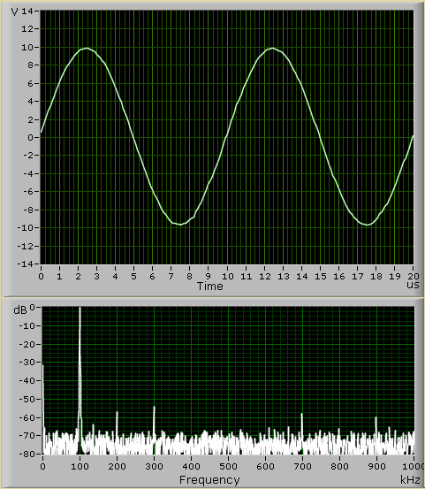
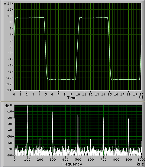
The oscillograms and spectrums of the typical signals are shown on figures 3 and 4. The measurement was made per one channel, the voltage range was switched to ±10V and the sampling rate was configured to 10MSPS. The first test signal is sine with amplitude of 10V and frequency of 100 kHz. The second test signal is square wave with porousness Q=2, 20V voltage swing, and frequency of 100 kHz. Test signals were generated by the low-frequency generator G3-112.
To compute the spectrum of signals 16384 samples were used. The Hanning window was used to suppress the spectrum spreading effect. On figures 3 and 4 the amplitude spectrums are shown, normalization was done by the maximum amplitude among the components of signal.
Measuring of signal in spectral domain allows extracting spectral component of the signal with the relative amplitude up to –60 dB.


The USB-analyzer of signals has following pa-rameters (table 1):
| Number of input channels | 4 |
| Input section bandwidth | 1 MHz |
| Vertical resolution | 8 bit |
| Sensitivity , full scale | ±1V, ±4V, ±10V, ±20V |
| Maximum sampling rate | 50 MHz |
| Minimum sampling rate | 100 kHz |
| Maximum memory per channel | 16384 samples |
| Bandpass flatness | 1dB |
Interface of connecting to PC is USB 2.0, signal analyzer feeds from power line of USB and is dis-pensed from auxiliary power source, and power consumption does not exceed 2,5 Watts.
Although maximal measuring range is ±20V, device is protected from the high voltage up to ±50V when it is switched on.
The developed measuring device is compact, multifunctional USB-analyzer of the signals with the functions of oscillograph, spectrum analyzer and digital voltmeter. This analyzer has four analog input channels with the bandwidth of 1 MHz. Input circuits are protected from the overcharge.
This device is intended to work with PC. It feeds from USB port. With PC the analyzer represents multifunctional hardware-software measuring solution. The capability of analyzer makes it possible to successfully use in educational laboratory lessons.
1. Mikushin A.V., Sedinin V.I., Malinkin V.B. Digital circuit technique. Monograph.
– Krasnoyarsk,Russia: Polycom, 2008. – 328p.
2. Fedosov V.P., Nesterenko A.K. Digital signal processing in LabVIEW // edited by Fedosov V.P.
– Moscow,Russia: DMC Progress, 2007. – 472p.: art.


Комментарии:
ср, 10/21/2015 - 06:41
Постоянная ссылка (Permalink)
Mikushin A.V., Sedinin V.I., Malinkin V.B. Digital circuit technique. Monograph
Where I may read this publication?
ср, 10/21/2015 - 13:02
Постоянная ссылка (Permalink)
Unfortunately, this publication is printed in limited edition and available only in print view in public technical librarues in Russia.